top of page

FINAL ADJUSTMENTS
The overcurrent works for the Vref being equal to 3.3[V], but now its time to make the reference around 1[V] with about a 10% error.
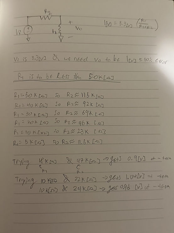
First thought went to creating a voltage divider to get a voltage drop and use that as our reference input.
I knew that I wanted to keep the highest amount of resistance below 50k[Ω} just because anything above would not be needed for this project. Starting at 50k and going down to 5k you can see the possible values for R2. Because I was using My universities electrical engineering stock room I was not able to find the exact values, and I wanted to keep this design simple so I did not want to use more than 2 resistors.
Working out the math, a 11k[Ω] resistor and a 25k[Ω] resistor got me a Vref value of 1.008[V], close to 1 and within our error range. Unfortunately the stock room did not have 25k[Ω] and being so close to a deadline I decided to redo the math and try to find a value that was the next best fit. Some quick math got me to 10k[Ω] and 24k[Ω], giving me an output of 0.96[V].
SIMULATIONS
With an idea in mind of what I needed and the math to tell me the values, it was time to simulate the circuit and see what was supposed to happen.
The first simulation shows what the Vref input will look like. According to LTspice, a 970.588[mV] input should be seen, and as a unit step function. The peek of the input is right about 970.618[mV], where as the the lowest is about 970.584[mV], so no need to think of it as a step function with a difference that small.
For the simulation as a whole, this shows that with the sin wave, blue input, having amplitudes of -3.3[V] and 3.3[V] and the Vref input, green input, being the 0.97[V] from above, the output describes what was wanted. Needing the circuit to read logic level high above the 1[V] (approximant) Vref input, just that was obtained. The red output shows that when the Vin goes above the 0.97[V] reference, it reads a logic level high, and when it sits below it reads a logic low.


BUILDING THE IMPROVED PROTOBOARD
Math and simulations went well so now it was time to apply this theory to a physical build. I had the protoboard from before so, I decided to skip the breadboard and add the improvements straight to the more sturdy design.
Adding the divider to the board went well and the last thing to do was to test this design and make sure it worked as intended.
bottom of page
